<?xml version="1.0" encoding="utf-8"?><feed xmlns="http://www.w3.org/2005/Atom" ><generator uri="https://jekyllrb.com/" version="3.10.0">Jekyll</generator><link href="https://bkcetinkaya.github.io/feed.xml" rel="self" type="application/atom+xml" /><link href="https://bkcetinkaya.github.io/" rel="alternate" type="text/html" /><updated>2025-12-06T16:15:02+00:00</updated><id>https://bkcetinkaya.github.io/feed.xml</id><title type="html">BKC</title><subtitle></subtitle><entry><title type="html">Designing a Common Emitter Amplifier With a Gain of 5</title><link href="https://bkcetinkaya.github.io/engineering/projects/2025/12/06/Designing-a-Common-Emitter-Amplifier-With-a-Gain-of-5.html" rel="alternate" type="text/html" title="Designing a Common Emitter Amplifier With a Gain of 5" /><published>2025-12-06T15:00:00+00:00</published><updated>2025-12-06T15:00:00+00:00</updated><id>https://bkcetinkaya.github.io/engineering/projects/2025/12/06/Designing%20a%20Common%20Emitter%20Amplifier%20With%20a%20Gain%20of%205</id><content type="html" xml:base="https://bkcetinkaya.github.io/engineering/projects/2025/12/06/Designing-a-Common-Emitter-Amplifier-With-a-Gain-of-5.html"><![CDATA[<p>First determine an acceptable Ic current, which is usually 1mA to 3mA. After that calculate the voltage drop at the Rc at Vdd/2. From that calculate \(Av = - {Rc \over Re1 + re}.\)
Determine the voltage divider resistors from: VE + 0.7</p>

<p><img src="/assets/av5.png" alt="Common Emitter" width="600" />
<img src="/assets/image.png" alt="Common Emitter" width="600" /></p>]]></content><author><name></name></author><category term="Engineering" /><category term="Projects" /><summary type="html"><![CDATA[First determine an acceptable Ic current, which is usually 1mA to 3mA. After that calculate the voltage drop at the Rc at Vdd/2. From that calculate \(Av = - {Rc \over Re1 + re}.\) Determine the voltage divider resistors from: VE + 0.7]]></summary></entry><entry><title type="html">Input and Output Impedance. Why is this so important?</title><link href="https://bkcetinkaya.github.io/engineering/projects/2025/09/22/Input-and-Output-Impedance.-Why-is-this-so-important.html" rel="alternate" type="text/html" title="Input and Output Impedance. Why is this so important?" /><published>2025-09-22T11:00:56+00:00</published><updated>2025-09-22T11:00:56+00:00</updated><id>https://bkcetinkaya.github.io/engineering/projects/2025/09/22/Input%20and%20Output%20Impedance.%20Why%20is%20this%20so%20important</id><content type="html" xml:base="https://bkcetinkaya.github.io/engineering/projects/2025/09/22/Input-and-Output-Impedance.-Why-is-this-so-important.html"><![CDATA[<p>If you are familiar with the BJT amplifier circuits, I am sure you heard the terms: “input impedance” , “output impedance”. But why do we even care? Lets take a look. But before I show you the circuits, I want to make things a bit clearer.
Lets assume we are designing a common-emitter amplifier to boost the weak input voltage that can be coming from a sensor. The modern IC sensors usually have low output impedance. And when you take this signal from the
sensor’s output to the input of your amplifier, it forms a voltage divider between the two. Therefore, if your amplifier has a low input impedance, you waste a lot of power and get a low voltage at the input of your amplifier,
and that is something that you dont want.</p>

<p>The voltage divider formula is as follows: Vout = Vsource * (R2/R1+R2). And if you do the calculations you may see that if R2 closer or smaller than R1, your Vout will be a fraction of Vsource. Take a look at the Simulation
in I setup in LTspice.</p>

<h3 id="first-case-r2-is-smaller-or-equal-to-r1">First Case (R2 is smaller or equal to R1)</h3>

<p><img src="/assets/1k-1k.png" alt="Schematic" width="500" /></p>

<p>
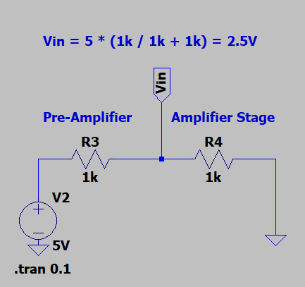
As you can see, of R2=R1=1K, you get 2.5V at the input of the amplifier stage. You basically waste energy for no reason.</p>

<h3 id="second-case-r2-is-significantly-larger-than-r1">Second Case (R2 is significantly larger than R1)</h3>

<p><img src="/assets/1k-100k.png" alt="Schematic" width="500" /></p>

<p>
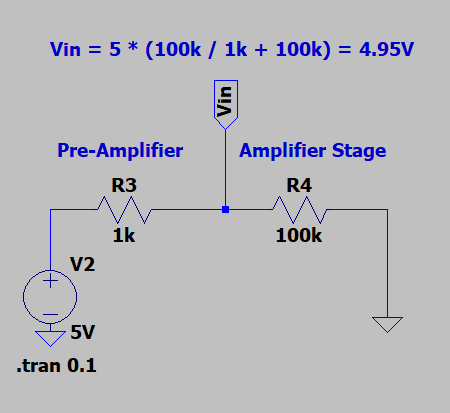
In this case, you get a voltage very close to the Source voltage which is visible in the schematic. You get 4.95V at the input of the amplifier stage.</p>

<p>Therefore, one must pay attention to the input and output impedances of the circuits. If the signal source has a low output impedance, the amplifier should have a high input impedance.</p>]]></content><author><name></name></author><category term="Engineering" /><category term="Projects" /><summary type="html"><![CDATA[If you are familiar with the BJT amplifier circuits, I am sure you heard the terms: “input impedance” , “output impedance”. But why do we even care? Lets take a look. But before I show you the circuits, I want to make things a bit clearer. Lets assume we are designing a common-emitter amplifier to boost the weak input voltage that can be coming from a sensor. The modern IC sensors usually have low output impedance. And when you take this signal from the sensor’s output to the input of your amplifier, it forms a voltage divider between the two. Therefore, if your amplifier has a low input impedance, you waste a lot of power and get a low voltage at the input of your amplifier, and that is something that you dont want.]]></summary></entry><entry><title type="html">Getting Good at Something is Very Slow and Painful</title><link href="https://bkcetinkaya.github.io/my/journals/2025/04/29/Getting-Good-at-Something-is-Very-Slow-and-Painful.html" rel="alternate" type="text/html" title="Getting Good at Something is Very Slow and Painful" /><published>2025-04-29T19:06:56+00:00</published><updated>2025-04-29T19:06:56+00:00</updated><id>https://bkcetinkaya.github.io/my/journals/2025/04/29/Getting%20Good%20at%20Something%20is%20Very%20Slow%20and%20Painful</id><content type="html" xml:base="https://bkcetinkaya.github.io/my/journals/2025/04/29/Getting-Good-at-Something-is-Very-Slow-and-Painful.html"><![CDATA[<p>As humans, we are programmed from birth to seek instant gratification. We instinctively avoid danger and tend to shy away from tasks that require time and effort. Well, that kind of thinking makes sense if you are a caveman just trying to make it through the day with enough to eat. Unfortunately, we live in the age of technology and you are not a caveman (I assume, since you are reading this), these flaws cause a lot of problems in our modern lives.</p>

<p>Let’s consider a case where you set unrealistic expectations (these are: assuming there won’t be any difficulty, it will take only a couple days, you will get good very quickly, there won’t be any pain or disappointment), unaware of the unconscious flaws in your thinking that I explained earlier. You set yourself a goal, you want to learn how to draw and you want to be really good at it. (You just watched Bob Ross got inspired by him, and you are fully motivated at least for now). Now you believe you will be able to draw like Bob Ross in a couple of days, or you believe that it won’t require much effort (This is literally what I have thought in the past). After trying it for the first time, you face the harsh reality that you can’t even draw a proper straight line yet alone a painting. You realize that it will take significantly more time and practice than you originally expected. Noticing how far reality falls short of your expectations, your motivation is destroyed and you quit in the first couple days.</p>

<p>Learning anything meaningful takes far more time than you expect. And not only is it a long journey, it also involves pain, disappointment and a lack of  gratification for a prolonged period. But if you begin with these things in mind, if you accept that it will not be easy and your progress will be very slow, you will eventually get there.
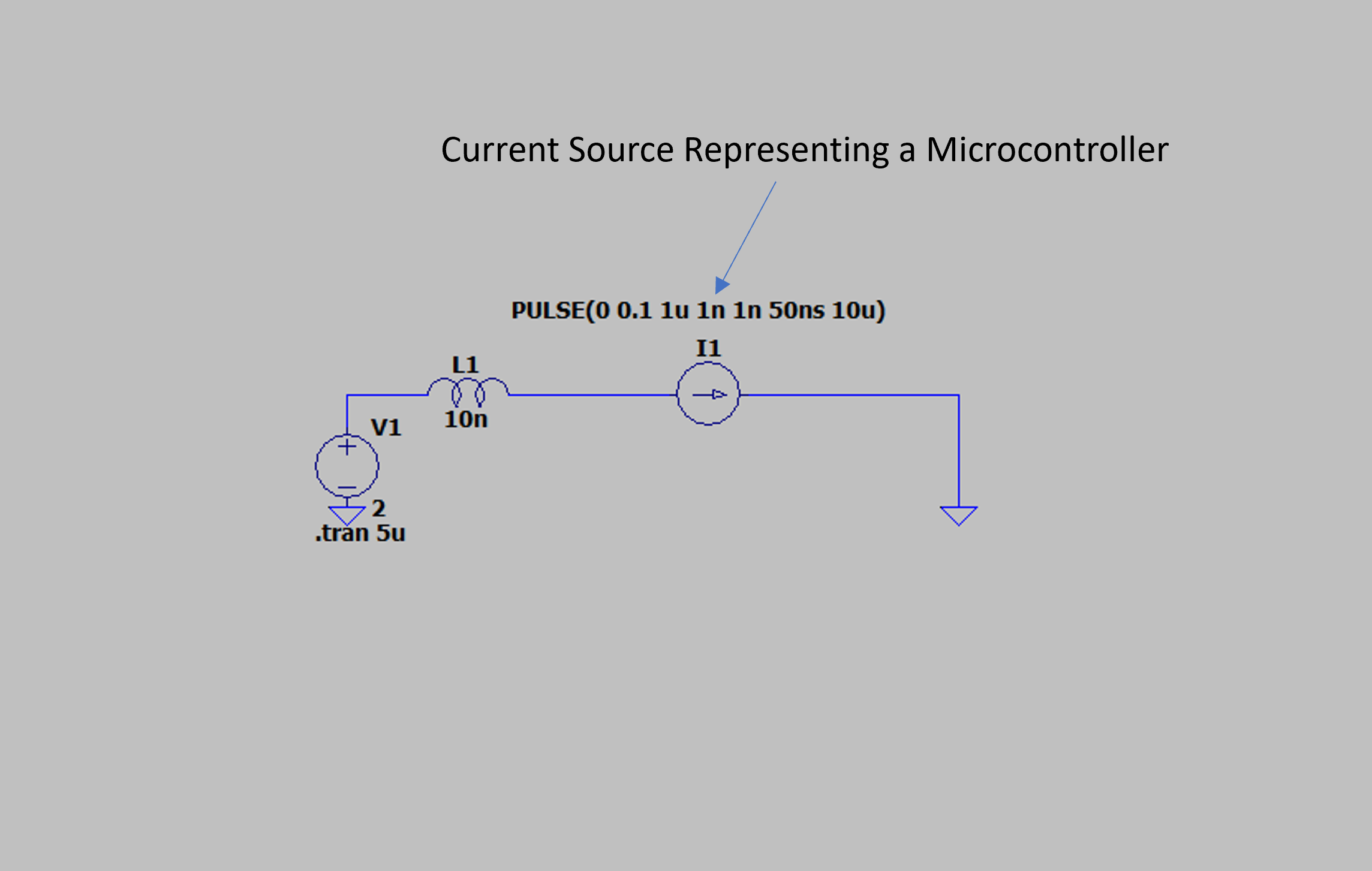
</p>]]></content><author><name></name></author><category term="My" /><category term="Journals" /><summary type="html"><![CDATA[As humans, we are programmed from birth to seek instant gratification. We instinctively avoid danger and tend to shy away from tasks that require time and effort. Well, that kind of thinking makes sense if you are a caveman just trying to make it through the day with enough to eat. Unfortunately, we live in the age of technology and you are not a caveman (I assume, since you are reading this), these flaws cause a lot of problems in our modern lives.]]></summary></entry><entry><title type="html">Decoupling Capacitors</title><link href="https://bkcetinkaya.github.io/engineering/projects/2025/02/12/Decoupling-Capacitors.html" rel="alternate" type="text/html" title="Decoupling Capacitors" /><published>2025-02-12T11:15:56+00:00</published><updated>2025-02-12T11:15:56+00:00</updated><id>https://bkcetinkaya.github.io/engineering/projects/2025/02/12/Decoupling%20Capacitors</id><content type="html" xml:base="https://bkcetinkaya.github.io/engineering/projects/2025/02/12/Decoupling-Capacitors.html"><![CDATA[<p>If you have designed pcb’s before, I am sure you have seen connecting ceramic capacitors to power terminal of microcontrollers. In this article, I will explain the purpose behind it.</p>

<p>We use decoupling capacitors to provide current almost intaneously to the part in the microcontroller where it is required. Current must be delivered in nanoseconds, but this cant be done by the power supply, because the wiring that connects power supply to the power terminal of the microcontroller has some inductance, and that resists to the sudden changes of current. This is where  capacitors come into play, we connect it as close as possible to the power terminal of a microcontroller, and the current is delivered almost instantenously.</p>

<p>
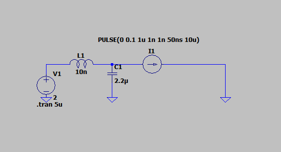
Lets look at two examples, one where we dont have a decoupling capacitor, and one we have a decoupling capacitor.</p>

<h2 id="without-a-decoupling-capacitor">Without a Decoupling Capacitor:</h2>

<p>
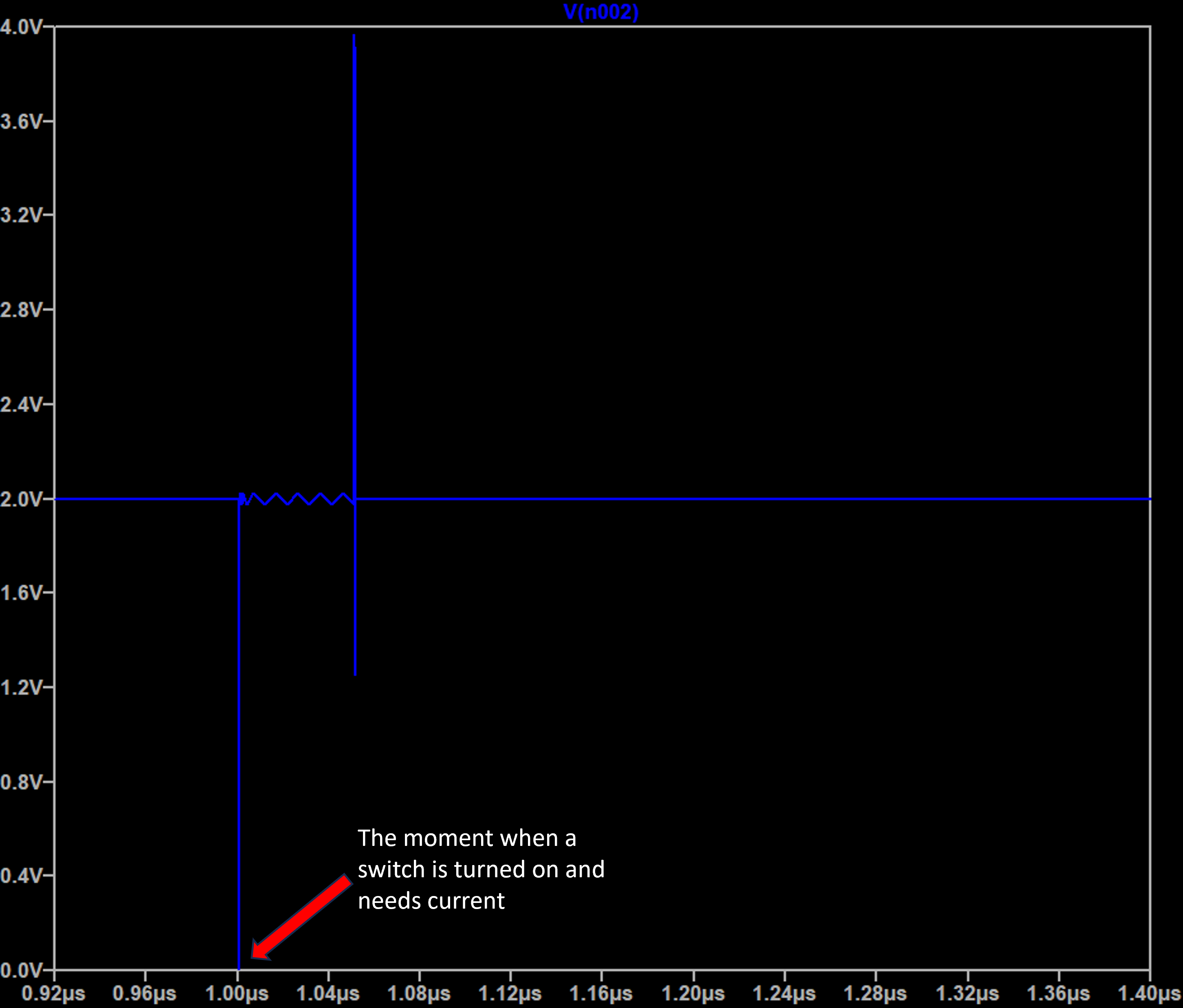
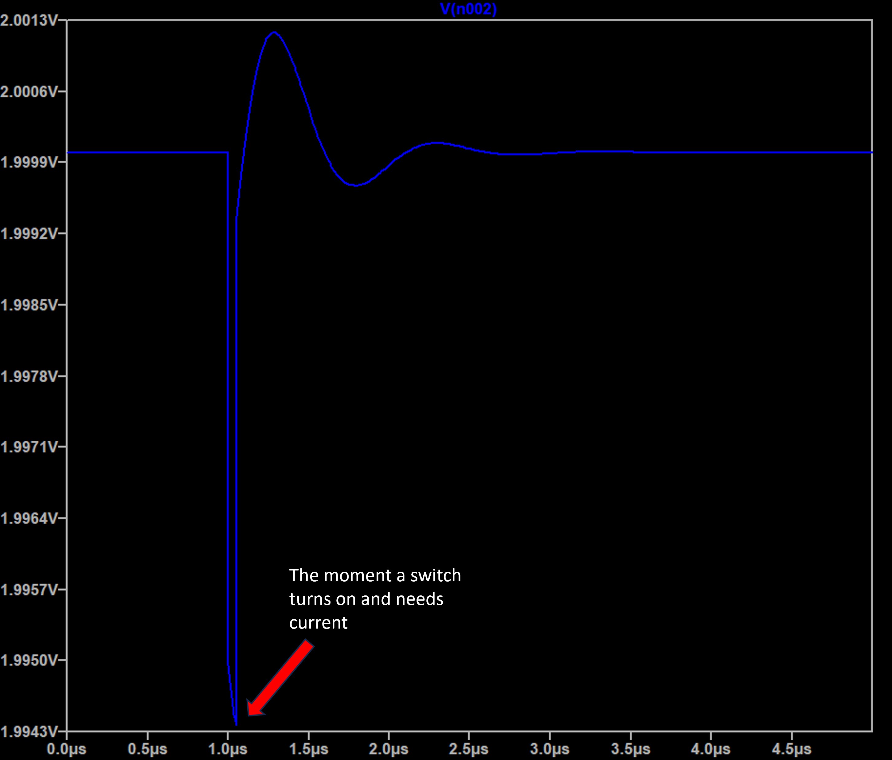
We connect power supply to our microcontroller, represented by a current source that requires 100mA when its turned on. The power line connecting the supply to the circuit has some inductance at nH level. Even if it seems small, it effects the circuits function significantly. See the schematic and the simulation results. The voltage at the pin of the current source oscillates a lot before it can stabilize at 2V, and it takes microseconds to stabilize, which is huge for a 100 Mhz microcontroller. This is caused by the inductance of the wiring, it resits sudden current changes. The power source wont be able to supply enough current in time, therefore microcontroller will malfunction.</p>

<p><img src="/assets/Withoutdcschematic.png" alt="Schematic" width="500" />
<img src="/assets/Withoutdc.png" alt="Schematic" width="500" /></p>

<h2 id="with-a-decoupling-capacitor">With a Decoupling Capacitor:</h2>

<p>Only difference now is we connect a capacitor between the power supply and the ground, differences are huge. When a sudden current is needed, capacitor can supply this current almost instanteosuly for a short amount of time until the power supply can start delivering current at required speed. See the differences in the simulation results, oscillations at the microcontroller terminal is almost non-existent.</p>

<p><img src="/assets/withdcschmatic.png" alt="Schematic" width="500" />
<img src="/assets/withdc.png" alt="Schematic" width="500" /></p>]]></content><author><name></name></author><category term="Engineering" /><category term="Projects" /><summary type="html"><![CDATA[If you have designed pcb’s before, I am sure you have seen connecting ceramic capacitors to power terminal of microcontrollers. In this article, I will explain the purpose behind it.]]></summary></entry><entry><title type="html">Botstrap Circuit For High Side MOSFETs</title><link href="https://bkcetinkaya.github.io/engineering/projects/2025/02/10/Botstrap-Circuit-For-High-Side-MOSFETs.html" rel="alternate" type="text/html" title="Botstrap Circuit For High Side MOSFETs" /><published>2025-02-10T20:27:56+00:00</published><updated>2025-02-10T20:27:56+00:00</updated><id>https://bkcetinkaya.github.io/engineering/projects/2025/02/10/Botstrap%20Circuit%20For%20High%20Side%20MOSFETs</id><content type="html" xml:base="https://bkcetinkaya.github.io/engineering/projects/2025/02/10/Botstrap-Circuit-For-High-Side-MOSFETs.html"><![CDATA[<p>Turning high side MOSFETs on and off (assuming you use an n-channel MOSFET to achieve fast switching due to their low RDS(on)) require bootstrap circuit to boost the gate voltage higher than the source voltage. We achieve this by utilizing a boostrap capacitor, diode and a BJT transistor.</p>

<h2 id="schematic-and-the-working-principle">Schematic and the Working Principle:</h2>

<p><img src="/assets/bootstrap.gif" alt="GPIO" width="3000&quot;, height:&quot;3000" /></p>

<p>In the inital state, the BJT is turned on. The gate of the high side MOSFET is at 0V. Bootstrap capacitor charges to VCC through the diode.
The load is connected to ground, so the source of the MOSFET is at ground potential.</p>

<p>When the BJT is turned off, capacitor discharges to the gate through the 1k resistor and turns the MOSFET on and we get 12V at the source terminal.
Since the capacitor and the source terminal are connected, we get a total of 24V at the gate terminal which turns the MOSFET fully on.
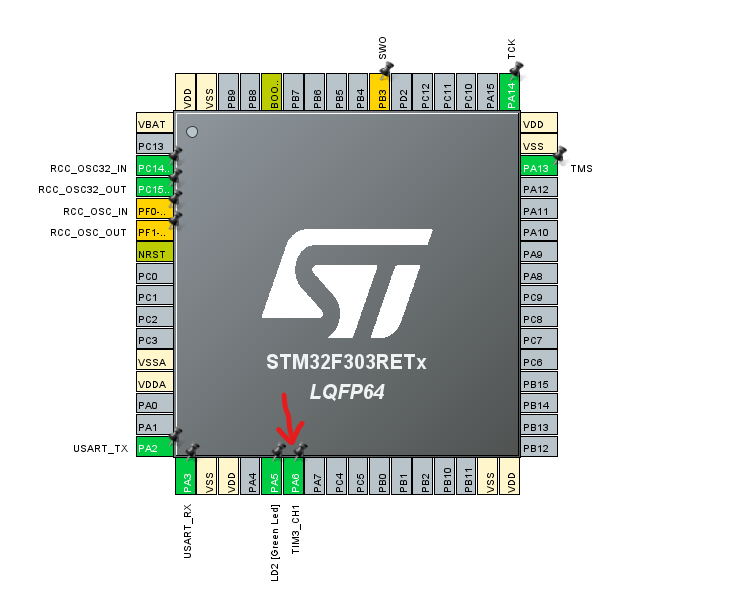
</p>]]></content><author><name></name></author><category term="Engineering" /><category term="Projects" /><summary type="html"><![CDATA[Turning high side MOSFETs on and off (assuming you use an n-channel MOSFET to achieve fast switching due to their low RDS(on)) require bootstrap circuit to boost the gate voltage higher than the source voltage. We achieve this by utilizing a boostrap capacitor, diode and a BJT transistor.]]></summary></entry><entry><title type="html">Generating PWM Signals With STM32 Microcontrollers</title><link href="https://bkcetinkaya.github.io/engineering/projects/2025/02/10/Generating-PWM-Signals-With-STM32-Microcontrollers-Copy.html" rel="alternate" type="text/html" title="Generating PWM Signals With STM32 Microcontrollers" /><published>2025-02-10T18:56:56+00:00</published><updated>2025-02-10T18:56:56+00:00</updated><id>https://bkcetinkaya.github.io/engineering/projects/2025/02/10/Generating-PWM-Signals-With-STM32-Microcontrollers%20-%20Copy</id><content type="html" xml:base="https://bkcetinkaya.github.io/engineering/projects/2025/02/10/Generating-PWM-Signals-With-STM32-Microcontrollers-Copy.html"><![CDATA[<p>Generating PWM signals with STM32 microcontrollers is straightforward. Just follow the instructions below:</p>

<h2 id="select-an-appropriate-gpio-pin">Select an appropriate GPIO pin:</h2>

<p>I chose the GPIO pin PA6 and set it to TIM_CH1, meaning Timer 3 and channel 1.</p>

<p><img src="/assets/pin selection.png" alt="GPIO" width="500" /></p>

<h2 id="activate-the-timer-channel-and-configure-settings">Activate the timer channel and configure settings:</h2>

<p>
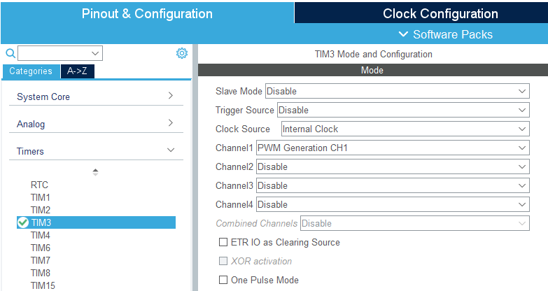
After activating the timer channel you set the pin to, configure the timer source to “Internal Clock” (Unless you want to use an external clock.) then set the Channel1 to “PWM Generation CH1”</p>

<p><img src="/assets/select timer channel.png" alt="TIMER3" width="500" /></p>

<h2 id="set-timer-parameters">Set Timer Parameters:</h2>

<p>Use the following formula to get your desired PWM frequency :</p>

<ul>
  <li>Your clock frequency / ( (prescaler + 1) x (ARR + 1) )</li>
  <li>Duty cycle is: (Pulse / ARR) x 100</li>
</ul>

<p><img src="/assets/timer configuration.png" alt="TIM" width="500" /></p>

<h2 id="example">Example:</h2>

<p>
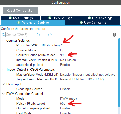
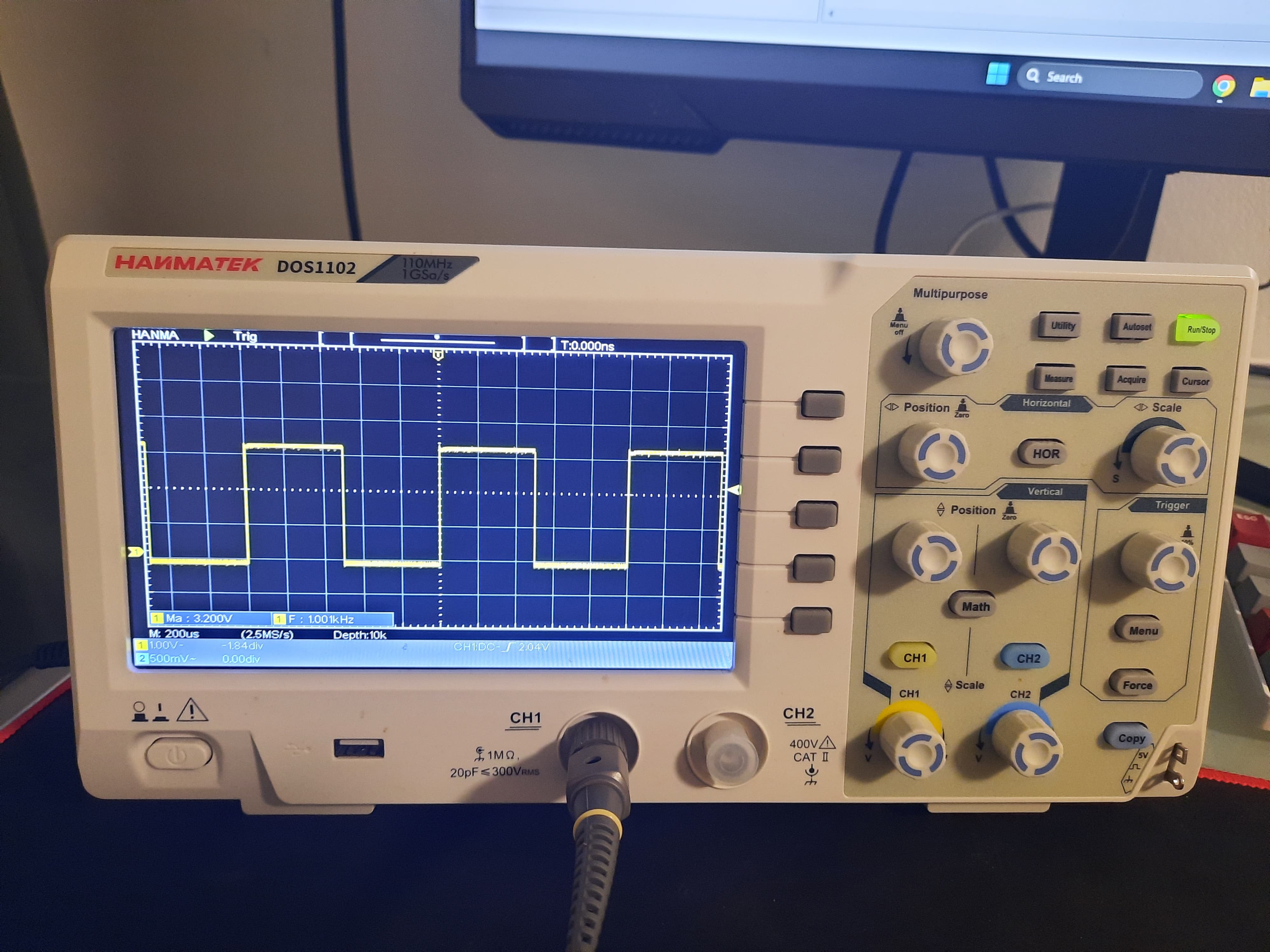
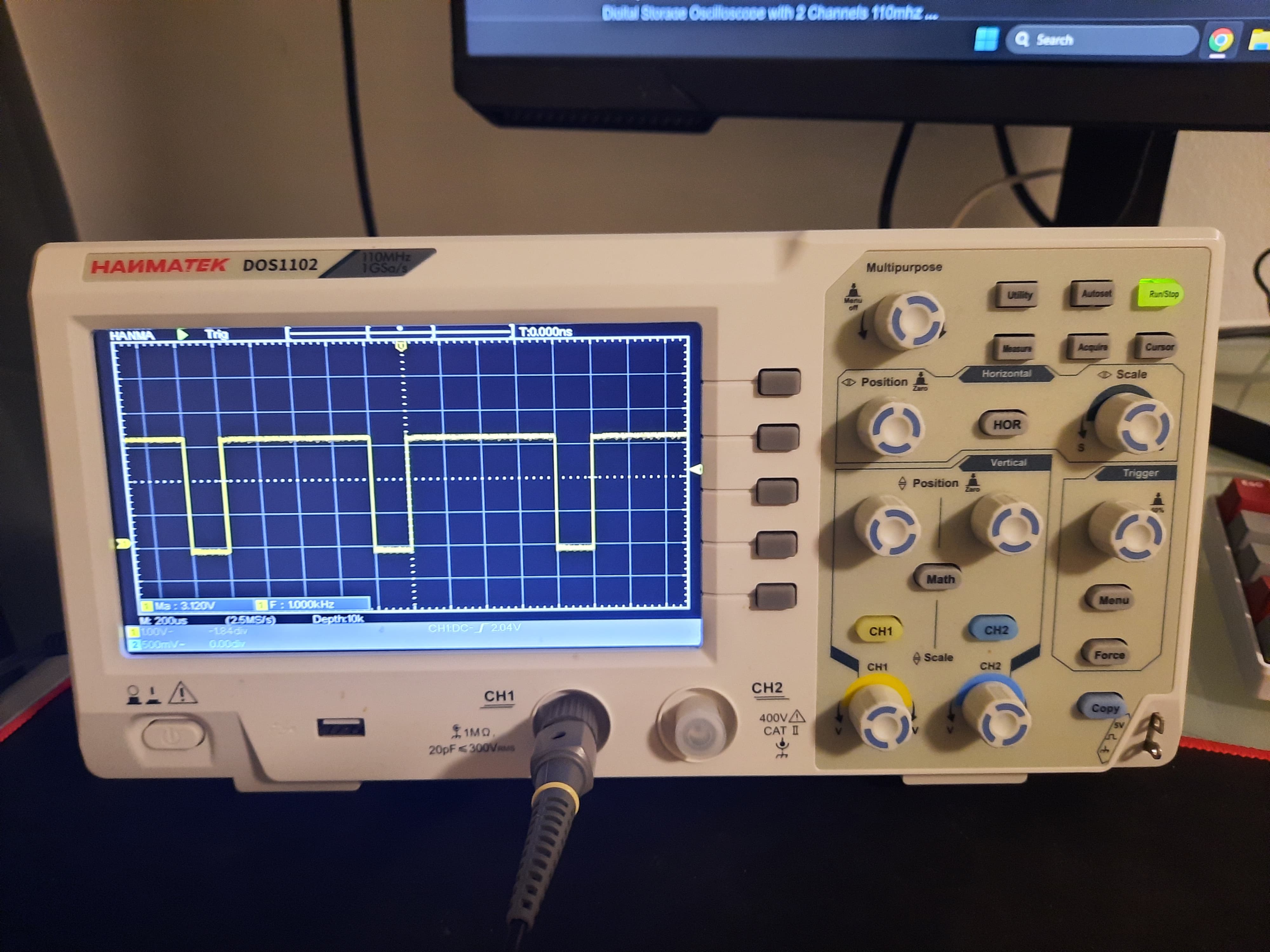
My clock source is running at 72MHz, I set the values so I get 80 percent and 50 percent duty cycles. These are the results on my oscilloscope:</p>

<p><img src="/assets/50duty.jpeg" alt="TIM" width="500" /></p>

<p><img src="/assets/80duty.jpeg" alt="TIM" width="500" /></p>]]></content><author><name></name></author><category term="Engineering" /><category term="Projects" /><summary type="html"><![CDATA[Generating PWM signals with STM32 microcontrollers is straightforward. Just follow the instructions below:]]></summary></entry><entry><title type="html">433 Mhz Bandpass Filter</title><link href="https://bkcetinkaya.github.io/engineering/projects/2024/12/24/433MHz-Bandpass-Filter.html" rel="alternate" type="text/html" title="433 Mhz Bandpass Filter" /><published>2024-12-24T18:15:56+00:00</published><updated>2024-12-24T18:15:56+00:00</updated><id>https://bkcetinkaya.github.io/engineering/projects/2024/12/24/433MHz%20Bandpass%20Filter</id><content type="html" xml:base="https://bkcetinkaya.github.io/engineering/projects/2024/12/24/433MHz-Bandpass-Filter.html"><![CDATA[<p>In the laboratory of my University, I was building a project where I needed to capture 433Mhz signals and measure the amplitude of the signals, But there was a small problem, 
the antenna that I was using, was picking up significant noise in the 1.3GHz range, which were affecting the overall amplitude of the received signal.</p>

<p>How to solve this? Of course with a bandpass filter!</p>

<p>
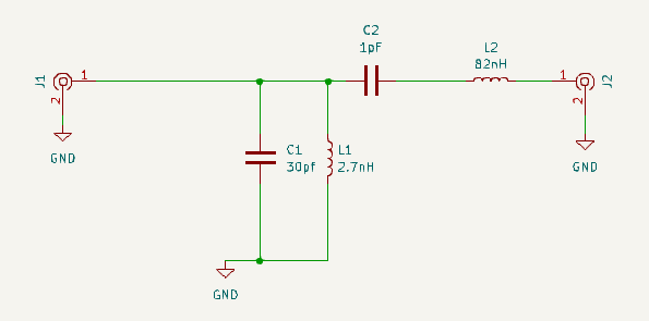
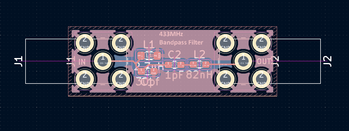
I designed the circuit using inductors and capacitors, created the schematic and also desinged the PCB as below:</p>

<h2 id="the-schematic">The Schematic:</h2>

<p><img src="/assets/Bandpass Schematic.png" alt="Schematic" width="500" /></p>

<h2 id="the-pcb-design">The PCB Design:</h2>

<p><img src="/assets/Bandpass Pcb.png" alt="PCB" width="500" /></p>

<p>
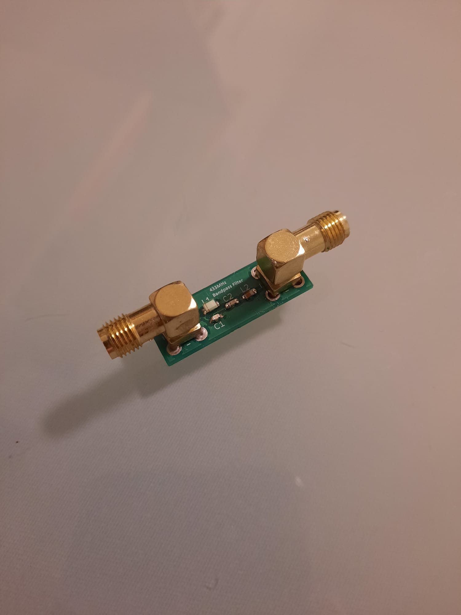
Even though soldering these incredibly small smd parts were too difficult, I have managed to solder them properly.</p>

<p>The pcb looks like this now with sma connectors on both ends:</p>

<p><img src="/assets/Bandpass Image.jpeg" alt="PCBbuilt" width="300" /></p>

<p>
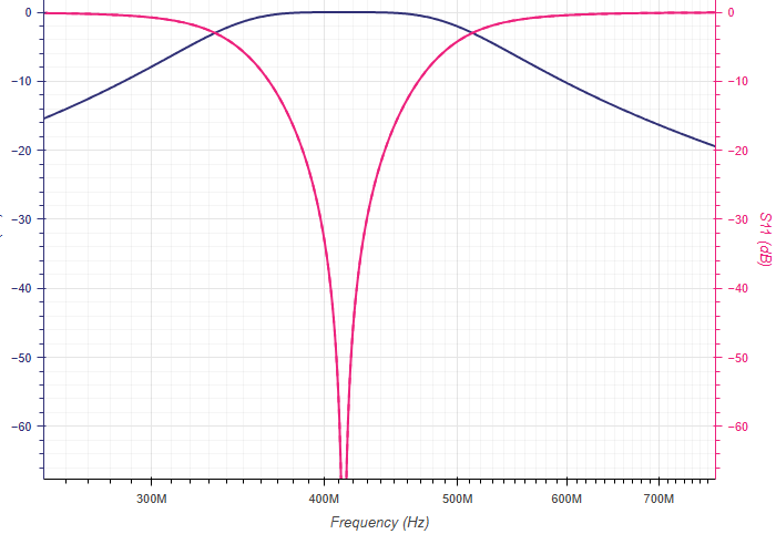
The S parameter shows that the filter is working as intended, having the lowest S11 point at around 400-450 Hz which is exactly what I needed.</p>

<h2 id="the-s-parameter-test">The S parameter Test:</h2>

<p><img src="/assets/Bandpass Filter S11 and S21.png" alt="Sparameter" width="500" /></p>

<p>To make sure, I connected a 1.3GHz signal and than a 433MHz signal to it to see if it is working properly, and saw that I now have a very low amplitude coming 
from the 1.3GHz signal which was exactly what I have wanted:</p>

<h2 id="output-when-13ghz-signal-is-applied">Output when 1.3GHz signal is applied:</h2>

<p><img src="/assets/Bandpass Response with 100Mhz.png" alt="1.3ghz" width="600" /></p>

<h2 id="output-when-433mhzhz-signal-is-applied">Output when 433MHzHz signal is applied:</h2>

<p><img src="/assets/Bandpass Response with 433Mhz.png" alt="433ghz" width="600" /></p>]]></content><author><name></name></author><category term="Engineering" /><category term="Projects" /><summary type="html"><![CDATA[In the laboratory of my University, I was building a project where I needed to capture 433Mhz signals and measure the amplitude of the signals, But there was a small problem, the antenna that I was using, was picking up significant noise in the 1.3GHz range, which were affecting the overall amplitude of the received signal.]]></summary></entry></feed>